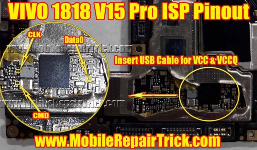
In this Article we will explain all about Vivo 1818 V15 Pro Isp Pinout. eMMC and eMCP memory are the standard in today’s smartphones, and the ISP practice enables examiners to directly recover the complete data without removing the chip and destroying the device. In-System Programming (ISP) allows communication to take place with a target chip without the need to remove it. The main advantage of this method is the possibility to communicate with a target chip eMMC or eMCP bypassing the CPU. It brings higher speed for data extraction compared with JTAG but it requires great soldering skills. ISP applied to forensics, is the practice of connecting to an eMMC or eMCP flash memory chip for the purpose of downloading a device’s complete memory contents.
VIVO 1818 V15 Pro Isp Pinout | VIVO V15 Pro Isp Pinout | VIVO 1818 Isp Pinout

What is ISP Pinout ?
ISP means “In-System Programming”.In-System Programming (ISP) allows communication to take place with a target chip without the need to remove it. The main advantage of this method is the possibility to communicate with a target chip eMMC or eMCP bypassing the CPU. It brings higher speed for data extraction compared with JTAG but it requires great soldering skills. ISP applied to forensics, is the practice of connecting to an eMMC or eMCP flash memory chip for the purpose of downloading a device’s complete memory contents.
eMMC and eMCP memory are the standard in today’s smartphones, and the ISP practice enables examiners to directly recover the complete data without removing the chip and destroying the device.ISP benefits the examiner who faces the challenges of tightening budgets, yet wants to expand their expertise in retrieving evidence from locked smartphones. A cost-effective technique, ISP provides examiners with the same results of a chip-off at a lower price-point.
Why do we need ISP Pinout ?
Just Like “Joint Test Action Group (JTAG)” there are specific contacts that will be of interest to the examiner. But unlike JTAG, the contacts are directly off the chip BGAs and do not go through the processor. Acquires data much faster than JTAG, enabling examiners to process more phones faster.
- CMD
- CLK
- DATA0
- GND
- VCC – Voltage Supply for Core (3,3V)
- VCCQ – Voltage Supply for I/O (1,8 – 3,3V)
The purpose of each signal is as follows:-
CLK : Clock signal for synchronization.Each cycle of this signal directs a one bit transfer on the command and either a one bit (1x) or a two bits transfer (2x) on all the data lines. The frequency may vary between zero and the maximum clock frequency
CMD : This signal is used to send the Host’s command and Device’s response.
Data0 : These are bidirectional data channels. The DAT signals operate in push-pull mode. Only the Device or the host is driving these signals at a time. By default, after power up or reset, only DAT0 is used for data transfer. A wider data bus can be configured for data transfer, using either DAT0-DAT3 or DAT0-DAT7, by the eMMC host controller. The eMMC Device includes internal pull-ups for data lines DAT1-DAT7. Immediately after entering the 4-bit mode, the Device disconnects the internal pull ups of lines DAT1, DAT2, and DAT3. Correspondingly, immediately after entering to the 8-bit mode the Device disconnects the internal pull-ups of lines DAT1–DAT7.
GND : VSS is the Ground for Core & VSSQ is the Ground for I/O.
VCC : VCC is the Power Supply for Core.
VCCQ : VCCQ is the Power Ssupply for I/O.
Click here for more information about ISP Pinout
VIVO 1818 V15 Pro Isp Pinout :
Subscribe our YouTube Channel for Free learning Mobile Repairing & Training.
Also see eMMC Service Tools for :
- Easy JTAG Plus Box
- Mipi Tester Box
- UFi Box
- Miracle Ninja Box
- Medus Pro 2 Box
Also see other models ISP Pinouts.
- Realme U1 RNX1831 ISP Pinout
- Samsung J210F Isp Pinout
- Samsung J500F Isp Pinout
- Realme 2 RMX1805 RMX1811 Isp Pinout
- Redmi Note 4 Isp Pinout
Also see other tools for Unlocking or Programming :
Download Files :
- Gsm Box & Dongle Setup
- ENG Firmware File
- Dump File
- Firmware
- EMMC FFU Firmware
- QCN File
- Baseband File
- EEPROM
- Unlock File
Buy GSM Box, Dongles, Activation & Tool’s from Store.GsmClinic.com
